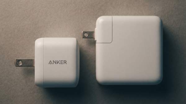
For any seasoned traveler, the ritual is familiar: the careful packing of a tangled nest of power bricks and cables, each dedicated to a specific device. For decades, the silicon-based chargers for our laptops, phones, and tablets have been a bulky, non-negotiable burden. The arrival of Gallium Nitride (GaN) technology has fundamentally altered this reality, offering chargers that deliver the same or even greater power from a dramatically smaller and lighter package. This transformation is not a simple feat of clever design but the direct result of GaN's superior properties as a semiconductor, allowing it to outperform the material that has defined electronics for generations.
At its core, GaN is a compound that conducts electricity far more efficiently than traditional silicon. This efficiency is the key to its revolutionary impact. When a charger converts AC power from a wall outlet to the DC power your devices need, inefficiency manifests as wasted energy, primarily in the form of heat. By generating significantly less heat, GaN allows engineers to design chargers with smaller, more densely packed components without the risk of overheating. The result is a new class of power adapter that is not only more portable but also cooler to the touch and more energy-efficient, making it an almost perfect solution for the modern traveler.
Understanding GaN: The Core Difference from Silicon
To appreciate the leap forward that Gallium Nitride represents, one must first understand the role of the semiconductor at the heart of every charger. These materials are the gatekeepers of electricity, precisely controlling the flow of current. For over half a century, silicon has been the undisputed workhorse of the electronics industry. It is abundant, reliable, and well-understood. However, silicon has inherent physical limitations, especially when it comes to managing high power in a small space. As our devices have become more power-hungry, the silicon-based chargers required to fuel them have remained stubbornly large.
Gallium Nitride enters as a challenger with a fundamentally different atomic structure that gives it a crucial advantage. This advantage is best quantified by a property known as the bandgap, which is the amount of energy required to make an electron in the material break free and conduct electricity. According to published lab measurements, GaN has a wide bandgap of 3.4 electron volts (eV), nearly triple the 1.1 eV bandgap of silicon. This seemingly abstract physical difference has profound, real-world consequences. A material with a wider bandgap can withstand much higher voltages and operate at higher temperatures before its electrical properties begin to break down.
For a power adapter, which must handle the full voltage from a wall outlet, this resilience is paramount. Because GaN can tolerate more electrical stress than silicon, the components built from it can be made significantly smaller while performing the same job, setting off a chain reaction of miniaturization throughout the charger's design.
GaN vs. Silicon: A Causal Chain of Benefits
The journey from a semiconductor's scientific properties to a tangible benefit in a traveler's bag follows a clear and direct path. GaN's inherent advantages over silicon are not just theoretical; they translate directly into engineering solutions that create a superior charging device. Each key property of GaN initiates a cascade of improvements, culminating in the compact, powerful chargers now available to consumers. The following table illustrates how this chain of cause and effect works.
| Physical Property (vs. Silicon) | Engineering Consequence | Traveler Benefit |
|---|---|---|
| Wider Bandgap (3.4 eV vs. 1.1 eV) | Components can withstand higher voltages and temperatures. This allows for a more compact internal layout with smaller parts packed closer together. | A significantly smaller and lighter charger that delivers the same amount of power, saving valuable space and weight in luggage. |
| Faster Switching Speed | GaN transistors can switch on and off much more quickly. This enables the use of smaller transformers and other passive components within the charger's circuitry. | The overall size of the charger is further reduced, contributing to its ultra-portable design and freeing up more space in a carry-on. |
| Higher Power Conversion Efficiency | Less electrical energy is lost as waste heat during the AC-to-DC conversion process. The charger runs cooler, requiring less bulky thermal management. | The charger remains cool to the touch even under heavy load, and a single compact unit can safely power multiple devices at once. |
The ability of GaN to switch between on and off states at a much higher frequency is a critical factor in reducing size. This faster switching allows designers to use smaller transformers, inductors, and capacitors—the passive components that are often the bulkiest parts of a traditional charger. Furthermore, the dramatic reduction in waste heat is a game-changer for design density. Silicon chargers must incorporate large heatsinks and significant empty space to prevent overheating. Because GaN runs cooler, components can be safely packed much closer together, enabling the final, compact form factor that travelers value.
The Traveler's Advantage: Real-World Benefits of GaN Chargers
The technical superiority of GaN translates into immediate and practical benefits for anyone on the move. The most significant of these is consolidation. A single, palm-sized GaN charger can now replace the collection of power bricks one might carry for a laptop, tablet, and smartphone. Many modern GaN chargers feature multiple ports, capable of intelligently delivering high-speed power to several devices simultaneously. This allows a traveler to shed the weight and untangle the mess of multiple single-purpose chargers, freeing up precious space in a carry-on or backpack. This versatility proves invaluable in common travel scenarios.
For a business traveler, a single GaN unit can keep a laptop, phone, and wireless earbuds powered up through a day of meetings, all from a single, often scarce, hotel or airport outlet. For vacationers, the space saved by leaving multiple chargers at home means more room for other essentials. The ability to efficiently power a high-draw device like a laptop alongside lower-power accessories from one compact source simplifies packing logistics and ensures all critical electronics remain ready for use. This solves the persistent problem of "low battery anxiety" that can shadow any trip.
Is a GaN Charger Right for Your Travel Kit?
The decision to invest in a GaN charger ultimately depends on a traveler's specific needs and priorities. The technology's core benefits—smaller size, lighter weight, and multi-device support—are most impactful for those who carry several electronic devices and are keen to minimize the bulk of their gear. While a person who travels with only a smartphone might not see a revolutionary change, the advantages become undeniable for anyone juggling the power demands of a modern digital life on the road. Consider upgrading to a GaN charger if you prioritize reducing luggage bulk, consolidating multiple chargers, and efficiently powering various devices from a single compact unit while traveling.
The ultimate payoff is a more streamlined and efficient packing system, where one small device capably handles the work previously done by three or more. A successful switch to this technology can be measured by a noticeable reduction in the number of power bricks and cables carried, and the ability to charge all essential devices simultaneously from one outlet.
Sources
- What Is a GaN Charger and How Is It Better? Complete Guide — Anker
- What is GaN Charger Technology? | Gallium Nitride — Verbatim EUROPE
- Everything you need to know about GaN chargers [PART 2] — Newell Pro - Camera Batteries, Chargers, LED lights and more - Power Brand
- What is a GaN Charger? Gallium Nitride Technology Explained — CairoVolt
- GaN Chargers for International Travel: Are They Worth It? — Ceptics
- Why You Need a GaN Travel Charger - Blog - - VCOM International Ltd
- Why are GaN Chargers Perfect for Travel and Mobile Work? — HyperShop.com